Field Emission Scanning Electron Microscopy Scanning Electron Microscopy (SEM) is a means of obtaining high-resolution, three-dimensional-like images of solid samples. Variations in the surface topography of a material are depicted as variations in gray level of the image. Details as small as 70 angstroms can be resolved on most samples. Dynamic experiments can be documented with the aid of a conventional video recorder. Energy Dispersive X-Ray Spectroscopy (EDS) extends the usefulness of SEM in that elemental analysis can be performed within regions as small as a few cubic micrometers. All elements from boron through the periodic table can be detected with sensitivities of approximately a few tenths of one percent. Learn More

What is Field Emission Scanning Electron Microscopy (FE-SEM)?

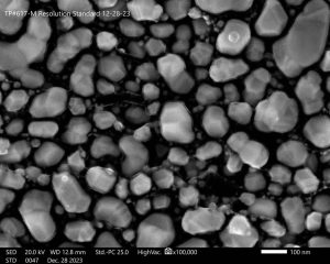
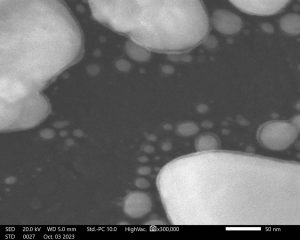
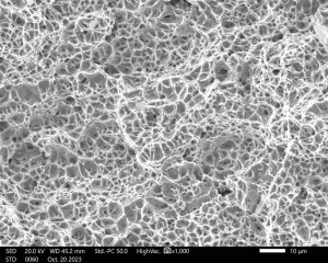
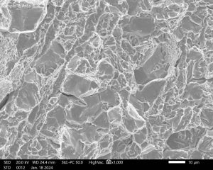
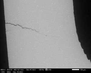
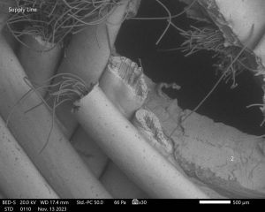
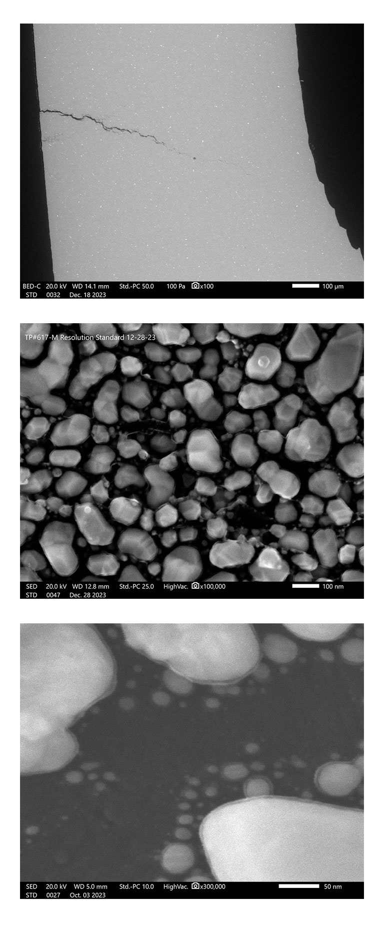
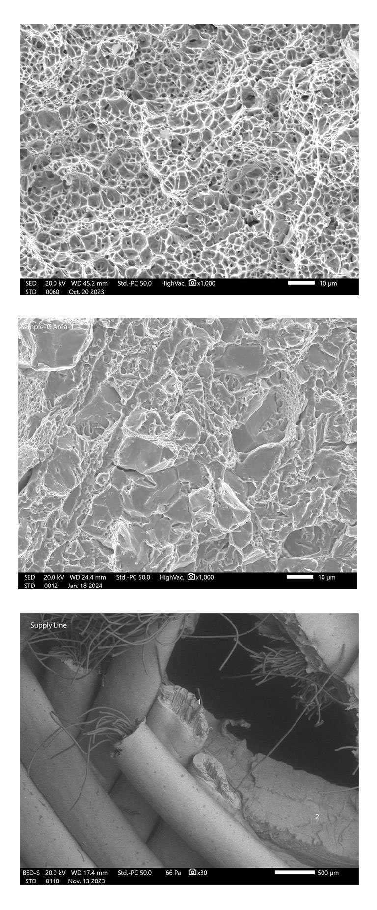
FE-SEM is a means for obtaining very high resolution three dimensional like images of solid samples. Variation in the surface topography of a material are depicted as variations in gray scale level of the image.

What Information can Field Emission Scanning Electron Microscopy (FE-SEM)?

FE-SEM can capture detailed images with a resolution as small as 1 nanometer on most samples. Micron Inc. utilizes a JEOL IT700HR/LA Field Emission instrument with low vacuum mode to routinely capture images of samples ranging in magnifications from 8X to 300,000X magnification. The JEOL IT700HR/LA FE-SEM has additional features, such as a large sample chamber that can accommodate samples with maximum dimensions of 126 mm (length) x 100 mm (width) x 80 mm(height)

What Materials can be analyzed using Field Emission Scanning Electron Microscopy (FE-SEM)?

Any solid materials such as metals, polymers, ceramics, pharmaceuticals, powders, fracture surfaces, and much more.

JEOL IT700HR
Sample Stage
JEOL IT700HR
Electron Gun

Ready To Get Started?

REQUEST YOUR QUOTE
TODAY